
Search
- Page Path
- HOME > Search
- [Korean]
- Study on the Preparation of TiO2 3D Nanostructure for Photocatalyst by Wet Chemical Process
- Duk-Hee Lee, Jae-Ryang Park, Chan-Gi Lee, Kyoung-Tae Park, Kyung-Soo Park
- J Korean Powder Metall Inst. 2020;27(5):381-387. Published online October 1, 2020
- DOI: https://doi.org/10.4150/KPMI.2020.27.5.381
- 1,302 View
- 7 Download
-
 Abstract
 PDF
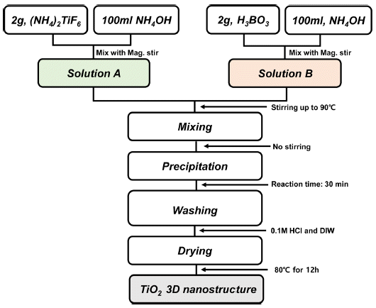
PDF In this work, TiO2 3D nanostructures (TF30) were prepared via a facile wet chemical process using ammonium hexafluorotitanate. The synthesized 3D TiO2 nanostructures exhibited well-defined crystalline and hierarchical structures assembled from TiO2 nanorods with different thicknesses and diameters, which comprised numerous small beads. Moreover, the maximum specific surface area of TiO2 3D nanostructures was observed to be 191 m2g-1, with concentration of F ions on the surface being 2 at%. The TiO2 3D nanostructures were tested as photocatalysts under UV irradiation using Rhodamine B solution in order to determine their photocatalytic performance. The TiO2 3D nanostructures showed a higher photocatalytic activity than that of the other TiO2 samples, which was likely associated with the combined effects of a high crystallinity, unique features of the hierarchical structure, a high specific surface area, and the advantage of adsorbing F ions.
- [Korean]
- Recent Developments in H2 Production Photoelectrochemical Electrode Materials by Atomic Layer Deposition
- Jeong Hwan Han
- J Korean Powder Metall Inst. 2018;25(1):60-68. Published online February 1, 2018
- DOI: https://doi.org/10.4150/KPMI.2018.25.1.60

- 1,161 View
- 2 Download
- 1 Citations
-
Abstract
PDF
The design and fabrication of photoelectrochemical (PEC) electrodes for efficient water splitting is important for developing a sustainable hydrogen evolution system. Among various development approaches for PEC electrodes, the chemical vapor deposition method of atomic layer deposition (ALD), based on self-limiting surface reactions, has attracted attention because it allows precise thickness and composition control as well as conformal coating on various substrates. In this study, recent research progress in improving PEC performance using ALD coating methods is discussed, including 3D and heterojunction-structured PEC electrodes, ALD coatings of noble metals, and the use of sulfide materials as co-catalysts. The enhanced long-term stability of PEC cells by ALD-deposited protecting layers is also reviewed. ALD provides multiple routes to develop improved hydrogen evolution PEC cells.
-
Citations
Citations to this article as recorded by
- Improved Interface and Electrical Properties by Inserting an Ultrathin SiO2 Buffer Layer in the Al2O3/Si Heterojunction
Doyeon Kim, Jae‐Young Choi, Sang Wook Ryu, Woo‐Byoung Kim
Advanced Functional Materials.2019;[Epub] CrossRef
- Improved Interface and Electrical Properties by Inserting an Ultrathin SiO2 Buffer Layer in the Al2O3/Si Heterojunction
- [Korean]
- Research Trends in Powder Materials for Solution-based Transparent Conducting Electrode
- Bon-Ryul Koo, Hyo-Jin Ahn
- J Korean Powder Metall Inst. 2017;24(2):153-163. Published online April 1, 2017
- DOI: https://doi.org/10.4150/KPMI.2017.24.2.153
- 1,008 View
- 4 Download
- 1 Citations
-
Abstract
PDF
Transparent conducting electrodes (TCEs) are attracting considerable attention as an important component for emerging optoelectronic applications such as liquid crystal displays, touch panels, and solar cells owing to their attractive combination of low resistivity (< 10-3 Ω cm) and high transparency (>80%) in the visible region. The solutionbased process has unique properties of an easy fabrication procedure, scalability, and low cost compared to the conventional vacuum-based process and may prove to be a useful process for fabricating TCEs for future optoelectronic applications demanding large scale and flexibility. In this paper, we focus on the introduction of a solution-based process for TCEs. In addition, we consider the powder materials used to fabricate solution-based TCEs and strategies to improve their transparent conducting properties.
-
Citations
Citations to this article as recorded by- Electrically conductive and anti-corrosive coating on copper foil assisted by polymer-nanocomposites embedded with graphene
Han Kim, Hyemin Lee, Hyo-Ryoung Lim, Hong-Baek Cho, Yong-Ho Choa
Applied Surface Science.2019; 476: 123. CrossRef
- Electrically conductive and anti-corrosive coating on copper foil assisted by polymer-nanocomposites embedded with graphene
- [Korean]
- Morphology Control of ZnO Nanostructures by Surfactants During Hydrothermal Growth
- Il-Kyu Park
- J Korean Powder Metall Inst. 2016;23(4):270-275. Published online August 1, 2016
- DOI: https://doi.org/10.4150/KPMI.2016.23.4.270
- 1,164 View
- 3 Download
- 1 Citations
-
Abstract
PDF
We report on an all-solution-processed hydrothermal method to control the morphology of ZnO nanostructures on Si substrates from three-dimensional hemispherical structures to two-dimensional thin film layers, by controlling the seed layer and the molar contents of surfactants during their primary growth. The size and the density of the seed layer, which is composed of ZnO nanodots, change with variation in the solute concentration. The ZnO nanodots act as heterogeneous nucleation sites for the main ZnO nanostructures. When the seed layer concentration is increased, the ZnO nanostructures change from a hemispherical shape to a thin film structure, formed by densely packed ZnO hemispheres. In addition, the morphology of the ZnO layer is systematically controlled by using trisodium citrate, which acts as a surfactant to enhance the lateral growth of ZnO crystals rather than a preferential one-dimensional growth along the c-direction. X-ray diffraction and energy dispersive X-ray spectroscopy results reveal that the ZnO structure is wurtzite and did not incorporate any impurities from the surfactants used in this study.
-
Citations
Citations to this article as recorded by- La-doped p-type ZnO nanowire with enhanced piezoelectric performance for flexible nanogenerators
Leeseung Kang, HyeLan An, Ji Young Park, Myung Hwan Hong, Sahn Nahm, Chan Gi Lee
Applied Surface Science.2019; 475: 969. CrossRef
- La-doped p-type ZnO nanowire with enhanced piezoelectric performance for flexible nanogenerators
- [Korean]
- Fabrication of ZnO Nanorod/polystyrene Nanosphere Hybrid Nanostructures by Hydrothermal Method for Energy Generation Applications
- Seong-Ho Baek, Il-Kyu Park
- J Korean Powder Metall Inst. 2015;22(6):391-395. Published online December 1, 2015
- DOI: https://doi.org/10.4150/KPMI.2015.22.6.391

- 1,236 View
- 3 Download
- 4 Citations
-
Abstract
PDF
We report on the successful fabrication of ZnO nanorod (NR)/polystyrene (PS) nanosphere hybrid nanostructure by combining drop coating and hydrothermal methods. Especially, by adopting an atomic layer deposition method for seed layer formation, very uniform ZnO NR structure is grown on the complicated PS surfaces. By using zinc nitrate hexahydrate [Zn(NO3)2 ·6H2O] and hexamine [(CH2)6N4] as sources for Zn and O in hydrothermal process, hexagonal shaped single crystal ZnO NRs are synthesized without dissolution of PS in hydrothermal solution. X-ray diffraction results show that the ZnO NRs are grown along c-axis with single crystalline structure and there is no trace of impurities or unintentionally formed intermetallic compounds. Photoluminescence spectrum measured at room temperature for the ZnO NRs on flat Si and PS show typical two emission bands, which are corresponding to the band-edge and deep level emissions in ZnO crystal. Based on these structural and optical investigations, we confirm that the ZnO NRs can be grown well even on the complicated PS surface morphology to form the chestnut-shaped hybrid nanostructures for the energy generation and storage applications.
-
Citations
Citations to this article as recorded by- Synthesis of Planar-Type ZnO Powder in Non-Nano Scale Dimension and Its Application in Ultraviolet Protection Cosmetics
Jung-Hwan Lee, Gun-Sub Lee, Eung-Nam Park, Dong-Hyeon Jo, So-Won Kim, Hee-Chul Lee
Materials.2023; 16(5): 2099. CrossRef - Rapid consolidation of nanostuctured WC-FeAl3 by pulsed current activated heating and its mechanical properties
In-Jin Shon, Seok-Jae Lee
International Journal of Refractory Metals and Hard Materials.2017; 65: 69. CrossRef - Fabrication of a Graphene/ZnO based p-n junction device and its ultraviolet photoresponse properties
Young-Tae Kwon, Sung-Oong Kang, Ji-Ae Cheon, Yoseb Song, Jong-Jin Lee, Yong-Ho Choa
Applied Surface Science.2017; 415: 2. CrossRef - Morphology Control of ZnO Nanostructures by Surfactants During Hydrothermal Growth
Il-Kyu Park
Journal of Korean Powder Metallurgy Institute.2016; 23(4): 270. CrossRef
- Synthesis of Planar-Type ZnO Powder in Non-Nano Scale Dimension and Its Application in Ultraviolet Protection Cosmetics
 First
First Prev
Prev

TOP
