
Search
- Page Path
- HOME > Search
- [English]
- Self-Assembled Monolayers in Area-Selective Atomic Layer Deposition and Their Challenges
- Si Eun Jung, Ji Woong Shin, Ye Jin Han, Byung Joon Choi
- J Powder Mater. 2025;32(3):179-190. Published online June 30, 2025
- DOI: https://doi.org/10.4150/jpm.2025.00094
- 6,504 View
- 249 Download
- 4 Citations
-
 Abstract
 PDF
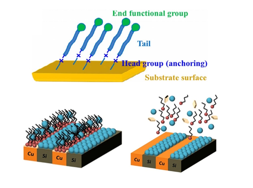
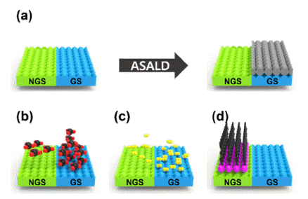
PDF - Area-selective atomic layer deposition (AS-ALD) is a bottom-up process that selectively deposits thin films onto specific areas of a wafer surface. The surface reactions of AS-ALD are controlled by blocking the adsorption of precursors using inhibitors such as self-assembled monolayers (SAMs) or small molecule inhibitors. To increase selectivity during the AS-ALD process, the design of both the inhibitor and the precursor is crucial. Both inhibitors and precursors vary in reactivity and size, and surface reactions are blocked through interactions between precursor molecules and surface functional groups. However, challenges in the conventional SAM-based AS-ALD method include thermal instability and potential damage to substrates during the removal of residual SAMs after the process. To address these issues, recent studies have proposed alternative inhibitors and process design strategies.
-
Citations
Citations to this article as recorded by
- Temperature-Dependent Surface Structural Change in Self-Assembled Monolayers Studied with Vibrational Sum-Frequency Generation and QM/MD Simulation
Hojeong Yoon, Saima Sadiq, Junhyeok Park, Kyungwon Kwak, Minhaeng Cho
The Journal of Physical Chemistry Letters.2026; 17(4): 1119. CrossRef - Vertically Aligned Micro‐ and Nanoneedles for Advanced Biomedical Applications: From Fabrication Strategies to Clinical Translation
Yerim Jang, Sowon Lee, Younghak Cho, Hyejeong Seong
Small Structures.2026;[Epub] CrossRef - Morphology dependent optical properties of inorganic–organic hybrid ZnO thin films
Saleem G. Rao, Muhammad B. Haider, Omar A. Saleh
The European Physical Journal Applied Physics.2026; 101: 5. CrossRef - Backbone‐Length‐Optimized Inhibitors Deliver Long‐Retention Selectivity in Area‐Selective ALD of VO2
Hae Lin Yang, Eun Chong Cho, Minchan Kim, Hye In Park, Ga‐young Lee, Seunghwan Lee, Beomseok Kim, Changhwa Jung, Youngkwon Kim, Jin‐Seong Park
Advanced Science.2026;[Epub] CrossRef
- Temperature-Dependent Surface Structural Change in Self-Assembled Monolayers Studied with Vibrational Sum-Frequency Generation and QM/MD Simulation
- [Korean]
- Recent Studies on Area Selective Atomic Layer Deposition of Elemental Metals
- Min Gyoo Cho, Jae Hee Go, Byung Joon Choi
- J Powder Mater. 2023;30(2):156-168. Published online April 1, 2023
- DOI: https://doi.org/10.4150/KPMI.2023.30.2.156
- 4,181 View
- 104 Download
- 2 Citations
-
Abstract
PDF
The semiconductor industry faces physical limitations due to its top-down manufacturing processes. High cost of EUV equipment, time loss during tens or hundreds of photolithography steps, overlay, etch process errors, and contamination issues owing to photolithography still exist and may become more serious with the miniaturization of semiconductor devices. Therefore, a bottom-up approach is required to overcome these issues. The key technology that enables bottom-up semiconductor manufacturing is area-selective atomic layer deposition (ASALD). Here, various ASALD processes for elemental metals, such as Co, Cu, Ir, Ni, Pt, and Ru, are reviewed. Surface treatments using chemical species, such as self-assembled monolayers and small-molecule inhibitors, to control the hydrophilicity of the surface have been introduced. Finally, we discuss the future applications of metal ASALD processes.
-
Citations
Citations to this article as recorded by- Ultrafast Synthesis of Molybdenum Disulfide via Flashlamp Annealing
Chan Hyeon Yang, Jaehak Lee, Jung Hwan Park
Journal of Powder Materials.2025; 32(6): 509. CrossRef - Selective Atomic Layer Deposition of Co Thin Films Using Co(EtCp)2 Precursor
Sujeong Kim, Yong Tae Kim, Jaeyeong Heo
Korean Journal of Materials Research.2024; 34(3): 163. CrossRef
- Ultrafast Synthesis of Molybdenum Disulfide via Flashlamp Annealing
 First
First Prev
Prev

TOP
