
Articles
- Page Path
- HOME > J Powder Mater > Volume 33(1); 2026 > Article
-
Research Article
- Structural, Electrical, and Optical Properties of Al–Mg Co-Doped ZnO Thin Films
- Jong-Mu Kim,†, Jun-Seo Park,†, Jun-Ha Lee, Min-Woo Kim, Jung-Woo Lee*
-
Journal of Powder Materials 2026;33(1):44-50.
DOI: https://doi.org/10.4150/jpm.2026.00031
Published online: February 28, 2026
Department of Materials Science and Engineering, Hongik University, Sejong, 30016, Republic of Korea
- *Corresponding author: Jung-Woo Lee E-mail: jungwoo@hongik.ac.kr
- †These authors contributed equally to this work.
© The Korean Powder Metallurgy & Materials Institute
This is an Open Access article distributed under the terms of the Creative Commons Attribution Non-Commercial License (http://creativecommons.org/licenses/by-nc/4.0/) which permits unrestricted non-commercial use, distribution, and reproduction in any medium, provided the original work is properly cited.
- 1,284 Views
- 23 Download
Abstract
- Al–Mg co-doped ZnO thin films were fabricated by a sol–gel spin-coating process to investigate the effect of dopant ratio on their structural, electrical, and optical properties. The total dopant concentration was fixed at 3 mol%, while the Al-to-Mg ratio was systematically varied in AlxMg0.03-xZn0.97O (0 ≤ x ≤ 0.03). X-ray diffraction analysis showed that the films maintained a hexagonal wurtzite structure with a preferred (002) orientation up to an Al concentration of 1.5 mol%, whereas higher Al contents resulted in a degradation of crystallinity due to exceeding the solid solubility limit of Al in the ZnO lattice. Hall effect measurements revealed a decrease in carrier mobility with increasing Al content, attributed to enhanced ionized impurity scattering, while the carrier concentration and electrical conductivity reached optimal values at an Al–Mg co-doping ratio of 1.5 mol%–1.5 mol%. All films exhibited high optical transmittance in the visible region, with the highest average transmittance of approximately 83% observed at the same composition. These results demonstrate that controlling the Al/Mg dopant ratio is crucial for optimizing the performance of ZnO-based transparent conducting oxide thin films.
- Al–Mg co-doped ZnO thin films were fabricated by a sol–gel spin-coating process with a fixed total dopant concentration. Optimizing the Al/Mg ratio revealed an optimal composition that balances crystallinity, electrical conductivity, and optical transparency, demonstrating strong potential for indium-free transparent conducting oxide applications.
Graphical abstract
- Transparent Conductive Oxides (TCOs) are pivotal materials that simultaneously exhibit high electrical conductivity and superior optical transparency within the visible light spectrum [1]. Due to these unique properties, TCO-based electrodes have been extensively utilized in a wide range of optoelectronic applications, including displays, solar cells, and touchscreens. Among various TCO candidates, Indium Tin Oxide (ITO) remains the most prevalent material owing to its exceptionally low resistivity (approximately 10-4 Ω•cm) and high transmittance exceeding 80–90% [1, 2]. However, the practical application of ITO in next-generation flexible electronics is significantly hindered by its inherent brittleness. Furthermore, the scarcity of indium poses critical economic and environmental challenges [2, 3].
- In response to these limitations, Zinc Oxide (ZnO) has emerged as a promising alternative, characterized by its natural abundance, cost-effectiveness, and environmental sustainability [2, 4]. Despite these advantages, undoped ZnO typically suffers from a relatively narrow bandgap and high resistivity compared to ITO, which necessitates strategic doping to enhance its performance as a TCO. Consequently, extensive research has been conducted on doping ZnO with group III elements, such as Aluminum (AZO) and Gallium (GZO), to improve electrical conductivity by increasing free carrier concentration [2, 4-6]. In parallel, Magnesium-doped ZnO (MZO) has been investigated to widen the bandgap and optimize optical properties [7].
- However, the incorporation of Mg often leads to a degradation in electrical conductivity. To mitigate this trade-off, co-doping strategies—specifically involving the simultaneous incorporation of group III elements and Mg (e.g., AlMgZnO or GaMgZnO)—have been proposed to achieve a synergistic balance between optical and electrical characteristics [8-11]. Nevertheless, existing literature on co-doped ZnO thin films has predominantly focused on varying the concentration of a single dopant while maintaining the other at a fixed level [8, 12]. Such an approach is inherently limited in its ability to fully capture the complex interactions and the continuous evolution of material properties, such as the trade-off relationship between transparency and conductivity [13].
- In the present study, we maintained a constant total dopant concentration of 3 mol% and systematically varied the Al-to-Mg ratio within the AlxMg0.03-xZn0.97O (0≤x≤0.03) system. The thin films were fabricated via a sol-gel spin coating method to facilitate a systematic analysis of their optical and electrical behaviors. This research aims to provide a comprehensive understanding of how continuous compositional transitions influence the overall performance of the films, thereby offering critical insights into the optimization of multi-component TCO materials. Our results demonstrate that the systematic transition of dopant ratios allows for the precise tuning of the bandgap and carrier transport mechanism, identifying an optimal Al/Mg composition that maximizes TCO performance for specific coating applications.
1. Introduction
- 2.1 Materials and Precursor Solution Preparation
- The precursor solutions were synthesized via a sol-gel process. Zinc acetate dihydrate (Zn(CH3COO)2•2H2O) was employed as the primary precursor and dissolved in 2-methoxyethanol to achieve a molar concentration of 0.75 M. The total volume of the solution was fixed at 12 mL for each sample. Monoethanolamine (MEA) was added to the solution as a stabilizer, maintaining a 1:1 molar ratio with the zinc precursor. In this process, MEA acts as a chelating agent that coordinates with Zn2+ ions, thereby enhancing the chemical stability and homogeneity of the precursor solution [14].
- For the fabrication of co-doped ZnO films, aluminum nitrate nonahydrate (Al(NO3)3•9H2O) and magnesium acetate tetrahydrate (Mg(CH3COO)2•4H2O) were utilized as Al and Mg dopants, respectively. To ensure a homogeneous mixture, Zn(CH3COO)2•2H2O was first dissolved, followed by the sequential addition of the Al and Mg sources. The total dopant concentration (Al+Mg) was fixed at 3 mol%, with the composition systematically varied according to the formula AlxMg0.03-xZn0.97O (0≤x≤0.03). All synthesized solutions were stirred for 2 h at room temperature and then aged for 48 h to ensure chemical stability.
- 2.2 Thin Film Deposition and Heat Treatment
- The thin films were deposited onto glass substrates (1×1 cm2). Prior to deposition, the substrates were cleaned ultrasonically in acetone and isopropyl alcohol (IPA) for 5 min each, followed by a 15-minute cleaning process using a UV-ozone cleaner. The films were fabricated using a spin-coating technique, and a schematic illustration of the overall fabrication procedure is shown in Fig. 1. Based on the optimized conditions, the spin speed was set at 4000 RPM for 30 s. After each coating cycle, the films were dried on a hot plate at 200 °C for 15 min to eliminate the solvent. This process was repeated five times to achieve the target film thickness. Finally, the deposited films were annealed in a furnace at 500 °C for 1 h.
- 2.3. Film Characterization
- The structural characteristics of the AlxMg0.03-xZn0.97O (0≤x≤0.03) films were analyzed using X-ray diffraction (XRD, SmartLab SE, Rigaku, Japan). The cross-sectional morphology and thickness were examined via field-emission scanning electron microscopy (FE-SEM, JSM-IT500HR, JEOL, Japan). Electrical properties, including carrier concentration, mobility, and resistivity, were evaluated through Hall effect measurements (HMS-3000, ECOPIA, Korea). Optical transmittance was measured in the range of 380–780 nm using UV-visible spectroscopy (UV-Vis, Evolution 220, Thermo Scientific, USA).
2. Experimental Section
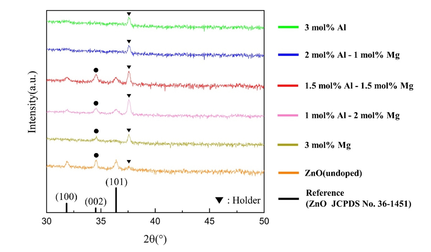
- 3.1 Structural Characteristics of Al–Mg Co-Doped ZnO Thin Films
- The crystalline structure and orientation of the AlxMg0.03-xZn0.97O (0≤x≤0.03) thin films were investigated via XRD analysis (Fig. 2). Undoped ZnO and Al-doped ZnO films with Al concentrations up to 1.5 mol% exhibited a pronounced (002) diffraction peak corresponding to the hexagonal wurtzite structure, indicating a strong preferential orientation along the c-axis perpendicular to the substrate. However, when the Al concentration exceeded 2 mol%, the ZnO (002) peak disappeared and no ZnO-related diffraction peaks were observed, suggesting a significant degradation of crystallinity. In contrast, films doped with 3 mol% Mg still exhibited a clear (002) peak, implying that the observed loss of crystallinity is primarily associated with excessive Al incorporation rather than Mg doping.
- This behavior can be explained by differences in ionic radii and solid solubility within the ZnO lattice. The ionic radii of Zn2+ (0.74 Å) and Mg2+ (0.72 Å) are comparable, resulting in minimal lattice distortion when Mg substitutes Zn sites [15]. In contrast, Al3+ has a much smaller ionic radius (0.53 Å), which induces substantial lattice strain upon substitution. Previous studies have reported that the solid solubility limit of Al in ZnO is approximately 1.3 mol%, beyond which Al atoms cannot be stably incorporated into the ZnO lattice [16]. In this context, the total dopant concentration in the present study was fixed at 3 mol% to minimize variations arising from overall dopant loading while enabling a controlled comparison of the relative contributions of Al and Mg near this solubility threshold. Consequently, excessive Al incorporation beyond this limit leads to severe lattice distortion and suppression of crystallization, resulting in amorphization of the film.
- The strong (002) preferential orientation observed in the crystalline films can be attributed to the thermodynamic stability of the (002) plane in the wurtzite structure, which possesses the highest atomic packing density and the lowest surface energy. During post-deposition annealing, atomic rearrangement preferentially occurs along the c-axis, making the intensity of the (002) diffraction peak a reliable indicator of crystallinity in ZnO-based thin films [17-19].
- 3.2 Electrical Transport Properties of Al–Mg Co-Doped ZnO Thin Films
- The electrical transport characteristics of the AlxMg0.03-xZn0.97O (0≤x≤0.03) thin films were evaluated by Hall effect measurements, and the corresponding results are summarized in Table 1. As the Al doping concentration increased from 0 to 2 mol%, the Hall mobility exhibited a monotonic decrease, declining from 258.1 to 13.9 cm2•V-1•s-1. This reduction in mobility can be attributed to the increased density of ionized impurity scattering centers caused by the substitution of Al³⁺ for Zn²⁺ [20], as well as the concomitant increase in carrier concentration, which enhances carrier–carrier scattering. When Al³⁺ ions substitute Zn²⁺ sites, they behave as ionized donors and generate positively charged scattering centers. The resulting Coulomb interaction between these centers and free electrons increases the probability of carrier scattering, shortening the carrier relaxation time and consequently lowering the Hall mobility. As the Al content increases, the density of these ionized impurities rises, leading to transport increasingly limited by ionized impurity scattering.
- In contrast, the carrier concentration and resistivity exhibited a non-monotonic dependence on the Al content. The carrier concentration increased with Al doping and reached a maximum value of 1.88 × 1015 cm-3 at an Al concentration of 1.5 mol% (x = 0.015), accompanied by a minimum resistivity of 5.89 × 10⁻¹ Ω•cm, indicating that Al acts as an effective donor in the ZnO matrix at moderate doping levels. However, when the Al concentration exceeded 1.5 mol%, the carrier concentration decreased, accompanied by a marked increase in resistivity and a further reduction in Hall mobility. This behavior suggests that excessive Al incorporation likely exceeds the solid solubility limit in ZnO [16], leading to Al segregation and/or the formation of electrically inactive defects or secondary phases, thereby reducing the effective donor concentration. According to the relation σ = neμ, the simultaneous decrease in carrier concentration and mobility at higher Al contents results in a pronounced degradation of electrical conductivity.
- Notably, despite the continuous decrease in Hall mobility with increasing Al content, the carrier concentration, and electrical conductivity exhibited optimal values at the composition of 1.5 mol% Al–1.5 mol% Mg. This composition represents an optimal balance between donor activation and impurity scattering effects, yielding superior electrical properties suitable for transparent conducting oxide applications.
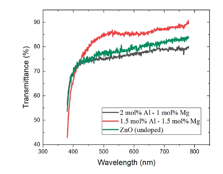
- 3.3 Optical Transmittance Characteristics of Al–Mg Co-Doped ZnO Thin Films
- The optical transmittance spectra of the AlxMg0.03-xZn0.97O (0≤x≤0.03) thin films are shown in Fig. 3 and Table 2. All fabricated films exhibited high optical transparency, with average transmittance values exceeding 75% in the visible wavelength range of 380–780 nm. These results indicate that Al–Mg co-doping does not significantly deteriorate the optical transparency required for transparent conducting oxide applications.
- Among the investigated compositions, the film with an Al concentration of 1.5 mol% (x = 0.015) exhibited the highest average transmittance, reaching approximately 83.0%. This behavior is consistent with the electrical characteristics, where the same composition showed optimized conductivity, suggesting that the dopant concentration optimized for electrical performance simultaneously preserves excellent optical transparency.
- In contrast, a noticeable reduction in transmittance was observed for films with higher Al content, particularly for the 2.0 mol% Al-doped sample (x = 0.02), which exhibited lower transmittance than even undoped ZnO. This degradation in optical performance is closely correlated with the structural deterioration observed at higher Al concentrations. Up to the onset of amorphization, Mg incorporation contributes to improved film density and reduced optical absorption, resulting in enhanced transmittance. However, when the Al concentration exceeds the amorphization threshold, increased structural disorder and defect-induced scattering counteract the beneficial effects of Mg doping, leading to reduced optical transparency. Although Mg incorporation is known to influence the bandgap of ZnO-based systems [7], the present study primarily focuses on optical transparency and electrical transport performance relevant to transparent conducting oxide applications; therefore, no quantitative bandgap analysis was conducted.
- It should be noted that optical transmittance is also influenced by surface roughness and film uniformity. In the present study, these factors were not quantitatively evaluated, and the sol–gel spin-coating process may inherently introduce thickness non-uniformity [21, 22]. Therefore, further investigations employing deposition techniques with higher uniformity, such as sputtering, along with quantitative surface roughness analysis, would provide deeper insight into the intrinsic optical behavior and enable more precise optimization of co-doping conditions.
- 3.4 Film Morphology and Thickness Optimization
- The cross-sectional morphology and thickness of the thin films were examined by SEM to identify fabrication conditions that satisfy the thickness requirements for high-performance ZnO-based transparent electrodes (Fig. 4). Two different fabrication conditions were compared: a precursor concentration of 0.3 M with seven spin-coating cycles (Fig. 4(a)) and a precursor concentration of 0.75 M with five spin-coating cycles (Fig. 4(b)).
- Previous studies have reported that the optimal thickness range for achieving favorable structural, electrical, and optical properties in ZnO-based transparent electrodes lies between 260 and 370 nm [23, 24]. Therefore, fabrication conditions capable of reproducibly achieving this thickness range are critical for reliable evaluation of co-doping effects.
- As shown in Fig. 4(b), the film fabricated using a precursor concentration of 0.75 M with five spin-coating cycles exhibited a thickness of approximately 280 nm, which falls squarely within the reported optimal range. In contrast, the film prepared using a lower precursor concentration required a higher number of coating cycles to approach a comparable thickness, indicating less efficient thickness control under these conditions.
- Accordingly, the fabrication condition of 0.75 M precursor concentration combined with five spin-coating cycles was selected as the standard process for subsequent Al–Mg co-doped ZnO thin films. This condition enables consistent fabrication of films within the optimal thickness window, thereby minimizing thickness-related variability and allowing the intrinsic effects of Al–Mg co-doping on structural, electrical, and optical properties to be evaluated more reliably.
3. Results and Discussion
- Al–Mg co-doped ZnO thin films were fabricated by a sol–gel spin-coating process as a potential indium-free alternative to ITO. Films were deposited under optimized conditions derived from undoped ZnO, ensuring reliable structural and electrical performance. XRD analysis showed that ZnO crystallinity with a strong wurtzite (002) preferred orientation was maintained up to an Al concentration of 1.5 mol%. At higher Al contents, the disappearance of ZnO diffraction peaks indicated amorphization caused by exceeding the solid solubility limit of Al in the ZnO lattice. This structural degradation was primarily attributed to Al incorporation rather than Mg. Hall measurements revealed a monotonic decrease in carrier mobility with increasing Al content due to enhanced ionized impurity scattering. Despite this trend, the carrier concentration and electrical conductivity reached their optimum at the co-doping composition of 1.5 mol% Al–1.5 mol% Mg, reflecting a balance between donor activation and crystallinity. Optical measurements showed high transparency in the visible region for all samples, with the highest average transmittance (~83%) observed at the same optimal co-doping ratio. Excessive Al doping led to reduced transmittance as a result of increased structural disorder and optical scattering. Overall, the Al–Mg co-doping ratio of 1.5 mol% Al–1.5 mol% Mg provides the most favorable combination of crystallinity, electrical conductivity, and optical transparency, demonstrating its strong potential as an ITO-free transparent conducting oxide for optoelectronic applications.
4. Conclusion
-
Funding
This work was supported by 2025 Hongik University Research Fund, and National Research Foundation of Korea(NRF) grant funded by the Korea government(MSIT)(RS-2024-00337423).
-
Conflict of Interest
The authors have no conflicts of interest to declare.
-
Data Availability Statement
The data that support the findings of this study are available from the corresponding author upon reasonable request.
-
Author Information and Contribution
Jong-Mu Kim, Jun-Seo Park: Undergraduate student; Conceptualization, Investigation, Data curation, Formal analysis, Writing – original draft.
Jun-Ha Lee, Min-Woo Kim: Undergraduate student; Conceptualization, Investigation, Data curation, Formal analysis
Jung-Woo Lee: Professor; Supervision, Writing – review & editing, Project administration.
-
Acknowledgments
None.
Article information


| Sample | Average Transmittance (%) |
|---|---|
| 2 mol% Al – 1 mol% Mg | 76.1 |
| 1.5 mol% Al – 1.5 mol% Mg | 83.0 |
| ZnO (undoped) | 78.2 |
- 1. H. Liu, V. Avrutin, N. Izyumskaya, Ü. Özgür and H. Morkoç: Superlattices Microstruct., 48 (2010) 458.Article
- 2. T. Minami: Semicond. Sci. Technol., 20 (2005) S35.Article
- 3. J. Liu, Y. Yi, Y. Zhou and H. Cai: Nanoscale Res. Lett., 11 (2016) 1.
- 4. Y. Liu, Y. Li and H. Zeng, ZnO-Based Transparent Conductive Thin Films: Doping, Performance, and Processing, College of Material Science and Technology, Nanjing University of Aeronautics and Astronautics, (2016).
- 5. N. Saxena, R. Sharma, A. Hussain, R. J. Choudhary, A. K. Debnath, O. P. Sinha and R. Krishna: Mater. Lett., 306 (2022) 130886.Article
- 6. D. Sun, C. Tan, X. Tian and Y. Huang: Materials, 10 (2017) 1039.
- 7. R. Kara, L. Mentar and A. Azizi: RSC Adv., 10 (2020) 40467.Article
- 8. S. H. Jeong, J. H. Park and B. T. Lee: J. Alloys Compd., 617 (2014) 180.Article
- 9. Y.C. Lin, T. Y. Chen, L. C. Wang and S. Y. Lien: J. Electrochem. Soc., 159 (2012) H599.Article
- 10. C. Y. Tsay, S. T. Chen and H. M. Tsai: Materials, 16 (2023) 6389.Article
- 11. I. Y. Kim, S. W. Shin, M. G. Gang, S. H. Lee, K. V. Gurav, P. S. Patil, J. H. Yun, J. Y. Lee and J. H. Kim: Thin Solid Films, 570 (2014) 321.Article
- 12. S. W. Shin, G. L. Agawane, I. Y. Kim, S. H. Jo, M. S. Kim, G. S. Heo, J. H. Kim and J. Y. Lee: Surf. Coat. Technol., 209 (2012) 180.
- 13. A. Mallick and D. Basak: Prog. Mater. Sci., 96 (2018) 86.Article
- 14. P. H. Vajargah, H. Abdizadeh, R. Ebrahimifard and M. R. Golobostanfard: Appl. Surf. Sci., 285 (2013) 732.Article
- 15. L. C. Yang, D. R. Jung, F. R. Po, C. H. Hsu and J. S. Fang: Coatings, 10 (2020) 708.Article
- 16. B. Mockenhaupt, J. K. Wied, S. Mangelsen, U. Schürmann, L. Kienle, J. S. auf der Günne and M. Behrens: Dalton Trans., 52 (2023) 5321.Article
- 17. M. Ohyama, H. Kouzuka and T. Yoko: Thin Solid Films, 306 (1997) 78.Article
- 18. K. Lim, M. A. Abdul Hamid, R. Shamsudin, N. H. Al-Hardan, I. Mansor and W. Chiu: Materials, 9 (2016) 300.Article
- 19. M. F. Malek, M. H. Mamat, Z. Khusaimi, M. Z. Sahdan, M. Z. Musa, A. R. Zainun, A. B. Suriani, N. D. M. Sin, S. B. A. Hamid and M. Rusop: J. Alloys Compd., 582 (2014) 12.Article
- 20. A. Wang, T. Chen, S. Wu, L. Lu, Y. Li, H. Chen and Y. Wang: Nanoscale Res. Lett., 10 (2015) 75.
- 21. S. Ippili, V. Jella, J. M. Lee, J. S. Jung, D. H. Lee, T. Y. Yang and S. G. Yoon: J. Mater. Chem. A, 10 (2022) 22067.Article
- 22. K. Vorotilov, V. Petrovsky and V. Vasiljev: J. Sol-Gel Sci. Technol., 5 (1995) 173.ArticlePDF
- 23. S. Mridha and D. Basak: Mater. Res. Bull., 42 (2007) 875.Article
- 24. V. Kumar, N. Singh, R. M. Mehra, A. Kapoor, L. P. Purohit and H. C. Swart: Thin Solid Films, 539 (2013) 161.Article
References
Figure & Data
References
Citations
 ePub Link
 Cite this Article
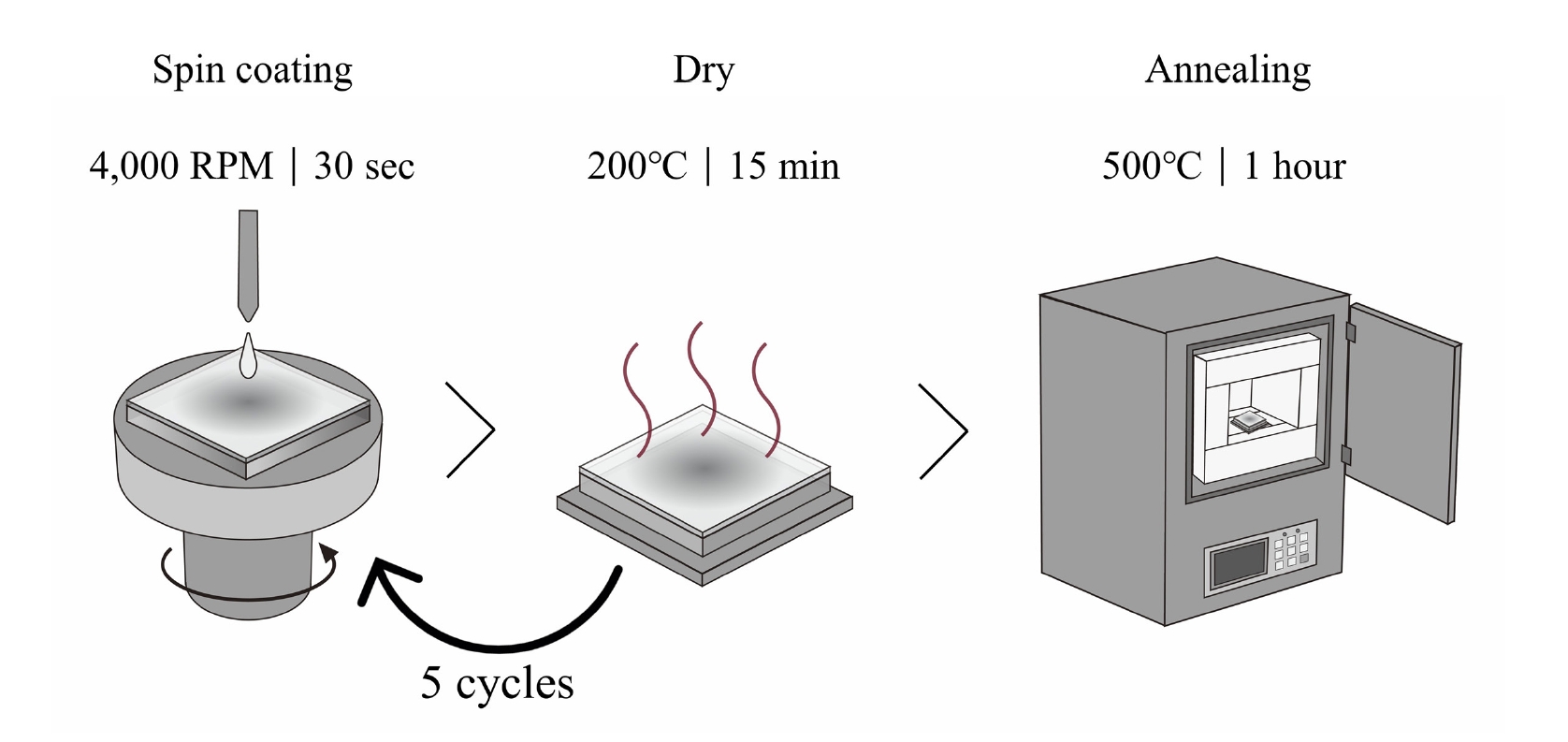


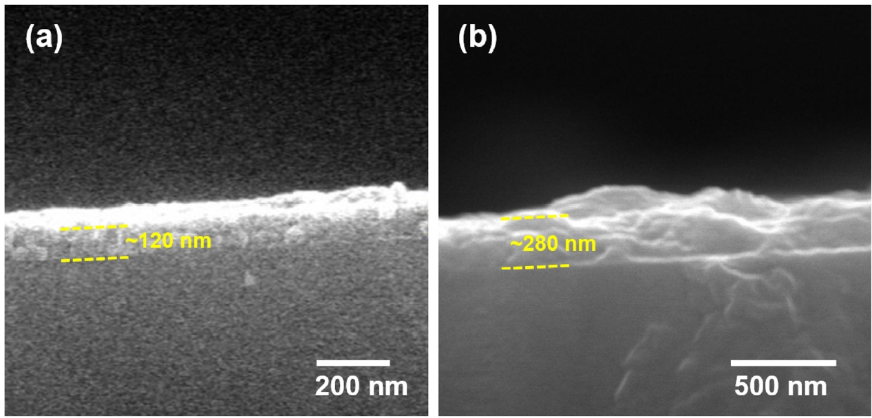
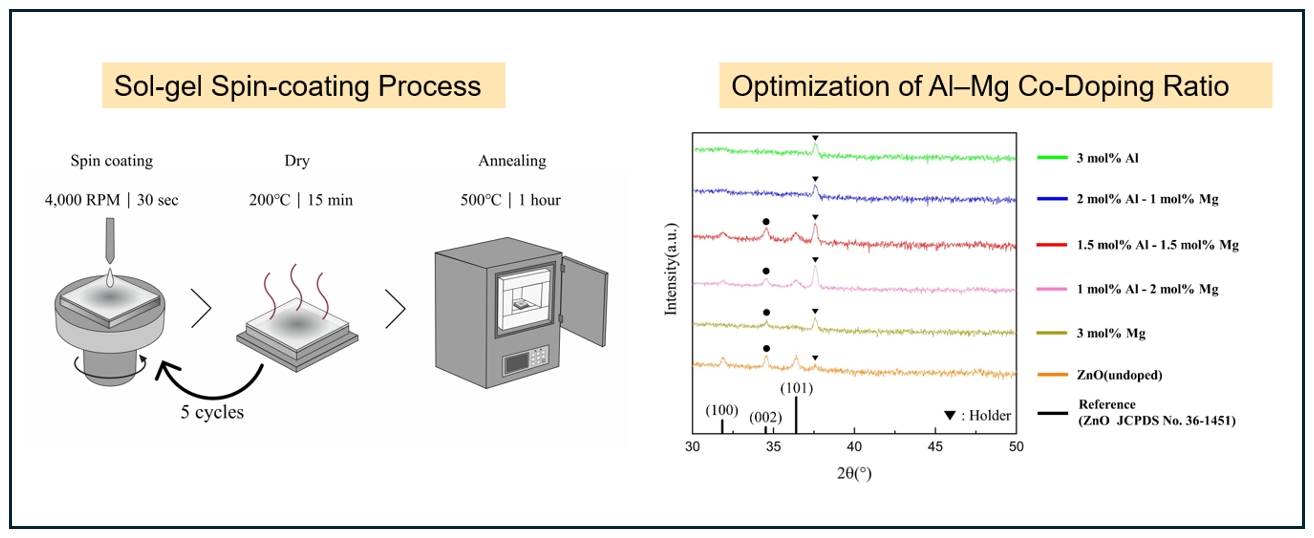
Fig. 1.
Fig. 2.
Fig. 3.
Fig. 4.
Graphical abstract
| Sample | Mobility (cm2/V·s) | Carrier Concentration (cm-3) | Resistivity (Ω·cm) | Conductivity (S/cm) |
|---|---|---|---|---|
| 2 mol% Al – 1 mol% Mg | 13.9 | 1.44×10¹⁵ | 3.11×10² | 3.21×10⁻³ |
| 1.5 mol% Al – 1.5 mol% Mg | 56.56 | 1.88×10¹⁵ | 5.89×101 | 1.70×10⁻² |
| 1 mol% Al – 2 mol% Mg | 81.3 | 4.31×10¹⁴ | 1.78×10² | 5.61×10⁻³ |
| ZnO (undoped) | 258.1 | 1.92×10¹² | 1.26×10⁴ | 7.93×10⁻⁵ |
| Sample | Average Transmittance (%) |
|---|---|
| 2 mol% Al – 1 mol% Mg | 76.1 |
| 1.5 mol% Al – 1.5 mol% Mg | 83.0 |
| ZnO (undoped) | 78.2 |
Table 1.
Table 2.
TOP
